PCB Technology
PCB Technology
Basics about the Printed Circuit Board
The printed circuit board is an essential component of power electronics and the direct interface to the high current contact. In power electronics projects, the selection of PCB technology is based on several criteria, including:
- Current carrying capacity and thermal management requirements.
- Experience of the layout designers / developers
- Available tools and their capabilities (ECAD / MCAD program, simulation etc.)
- Cost for prototypes and series volume
- Offer / portfolio of preferred PCB suppliers
- Third party experiences / references
The nomenclature used by PCB manufacturers is often not inconsistent. For example, different terms are used for embedded solid copper blanks. In the following sections, we use "copper-inlays" as a collective term. In addition, the distinction between standard and thick copper technology is not uniform. Manufacturers offering special technology sometimes refer to copper thicknesses above 70 µm as thick copper technology, while others refer to thicknesses up to 200 µm as standard.
PCB structure types compared
| Structure type | Standard | Thick copper | Wirelaid® | Copper inlays | IMS |
|---|---|---|---|---|---|
Structure |  |  |  |  |  |
Description | Copper structure: up to 70 µm Material: FR4 TG value: Standard TG 135 to High TG 170 |
| Standard printed circuit board with copper wire welded on copper foil | Standard printed circuit board with partially embedded or pressed-in solid copper inlays | IMS Copper layer on metallic carrier separated by a dielectric |
Notes |
|
|
|
|
|
Printed circuit board types in detail: from the standard structure to the IMS variant

Printed circuit board designs with up to 70 µm copper structure are designated as standard. Structures range from the simple two-layer to the multilayer boards. They are offered in the standard FR4 material, a flame-retardant composite material made of epoxy resin and fiberglass. TG values range from standard with TG 135 to high with TG 170, which is an established technology offered by many manufacturers. Due to the high currents in power electronics, the structure has limited applicability.

Thick copper is when the copper cladding ranges from 105 µm to 400 µm. This structure is also offered from standard FR4 with TG 135 up to TG 170. Our experience shows that the majority of high current projects can be realized with 105 µm copper claddings on inner layers.
Extensive simulations and calculations are available for this PCB structure and many PCB manufacturers can be accessed. As with the standard structure, the layout can be freely designed and the structure can be multilayer.

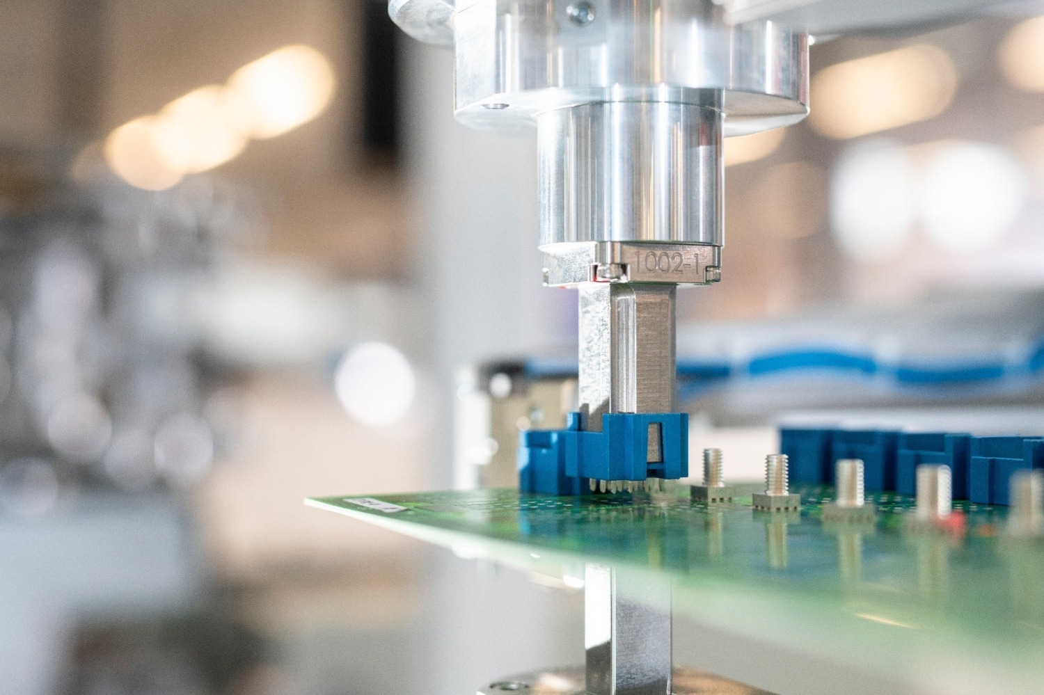
Wirelaid PCBs have a copper wire welded to the copper foil and embedded in the prepreg. High currents can be carried by the copper wire, but the current carrying capacity is limited due to the laying of the copper wire. Direct contact to the copper wire is not possible with press-fit technology.
New! Technology with thicker wires for higher currents

Solid copper inlays are sometimes embedded or pressed into a standard printed circuit board. This addition allows very high currents to be conducted locally, and the high thermal conductivity of the copper optimizes heat dissipation. Small, round copper inlays are used for heat dissipation (heat sink) under components.
Typically, this design requires an additional joining process during PCB manufacture and the copper inlays must be manufactured separately. Direct contacting of the copper inlays using press-fit technology is possible, but may require tuning depending on the structure.

Insulated Metal Substrate (IMS) printed circuit boards have a metal substrate (usually aluminum) separated from the copper layer by a dielectric. This structure allows efficient thermal dissipation of the power loss. However, the conductor pattern can only be applied on one side, and the metal substrate does not allow press-fit contacting.
Design guidelines for PCB layout

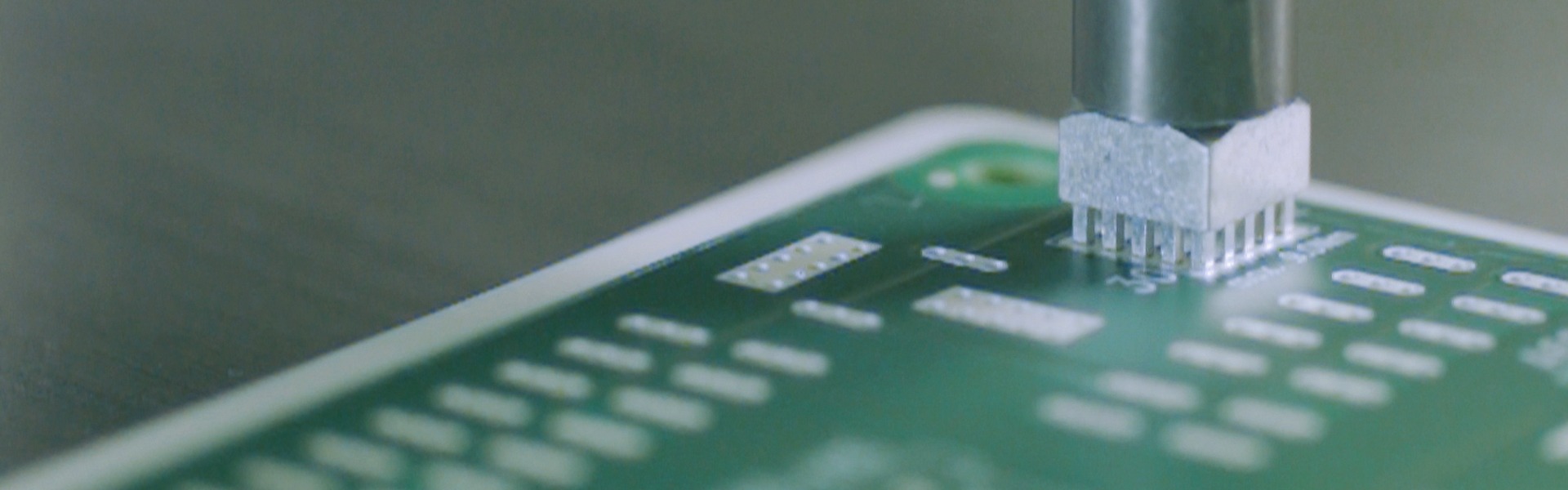
- The PCB should be > 1.5 mm thick to achieve the specified press-in and holding forces.
- For thinner PCBs, ensure that the specified holding force of at least 40 N per pin is achieved.
- Powerelements should not be placed on the edge or in a corner to achieve optimum current carrying capacity and thermal management.
- If the Powerelement must be placed on the edge of the PCB, the distance between the edge of the PCB and the through hole for the pin must be > 1.6 mm.
- The distance between the Powerelements must be selected such that it is possible to guide the tool required for the press-fit process.
- A distance of > 3 mm from SMD components must be maintained to prevent damage to sensitive components.
- The entire surface of the pad for the Powerelement must be exposed in the solder resist and not just individual pads.
- The recommended distance between a conductor track and the pad of the Powerelement is > 0.7 mm.
In general, the following applies: The PCB holes must be drilled according to the manufacturer's specifications for the high-current contact.
Larger holes may be required for PCB thicknesses > 3.2 mm, PCB materials with a high TG value or a total copper thickness > 0.8 mm.
")
- The PCB thickness should be > 1.0 mm.
- The solder pad is full-surface, but there should be ridges between the holes in the solder resist.
- Powerelements should not be placed at the edge or in a corner for optimal current carrying capacity and thermal management.
- The recommended distance between a conductor track and the solder pad of the Powerelement and SMD components is > 0.7 mm.
- The holes for the PCB are to be drilled according to the manufacturer's specifications.
- Only the final diameter of the through-hole plating is relevant.
- A sufficient residual ring around the holes must be taken into account to ensure the holding force.

As for THT and THR components, adapted layout rules also apply to SMD components:
- PCB thickness should be > 1.0 mm.
- Powerelements should not be placed at the edge or in a corner to achieve optimum current carrying capacity and thermal management.
- The recommended distance between a conductor track and the solder pad of the Powerelement and other SMD components is > 0.7 mm.
- The footprint must be designed according to the manufacturer's specifications.
- For SMD components, the solder pad should be approx. 1 mm larger than the footprint of the component.
- Vias for connecting the individual layers are to be placed circumferentially outside the solder pad or inside the solder pad as filled and sealed vias according to IPC 4761 Type 7.
- The paste printing shall be carried out with lands according to the manufacturer's instructions.
Drill hole specifications

For press-fit technology, the PCBs must be designed according to the Würth Elektronik ICS Press-Fit specification. Special attention must be paid to the drill diameter and copper thickness. The optimum PCB thickness is between 2.0 mm and 3.2 mm, but must be at least 1.5 mm. Proven finishes include immersion tin (preferred), immersion silver, immersion gold, HAL and lead-free HAL.

Copper sleeves for mounting in PCBs are as follows:
- Drill diameter and end diameter will vary depending on pitch and/or PCB surface. The values that need to be adhered to can be found in the respective drilling diagram.
- The drill bit must match to the nominal diameter of the hole.
- Copper build-up must be at least 25 µm at each point.
- Average copper thickness in the sleeve 30 µm all around, max. 60 µm.
- The final copper thickness of the board must be at least 70 µm to ensure this deposition.
- Final diameter with tolerances can be adjusted if required.
- Product specific vias must be observed.
- Specified press-in forces must be observed.